
Author Affiliations
Abstract
1 Zhejiang University, College of Information Science and Electronic Engineering, State Key Laboratory of Modern Optical Instrumentation, Key Laboratory of Micro-Nano Electronics and Smart System of Zhejiang Province, Hangzhou, China
2 Westlake University, School of Engineering, Key Laboratory of 3D Micro/Nano Fabrication and Characterization of Zhejiang Province, Hangzhou, China
3 Institute of Advanced Technology, Westlake Institute for Advanced Study, Hangzhou, China
4 Institute of Microelectronics of the Chinese Academy of Sciences, Beijing, China
5 Peking University, School of Physics, Frontiers Science Center for Nano-optoelectronics, State Key Laboratory for Mesoscopic Physics, Beijing, China
Optical neural networks (ONNs), enabling low latency and high parallel data processing without electromagnetic interference, have become a viable player for fast and energy-efficient processing and calculation to meet the increasing demand for hash rate. Photonic memories employing nonvolatile phase-change materials could achieve zero static power consumption, low thermal cross talk, large-scale, and high-energy-efficient photonic neural networks. Nevertheless, the switching speed and dynamic energy consumption of phase-change material-based photonic memories make them inapplicable for in situ training. Here, by integrating a patch of phase change thin film with a PIN-diode-embedded microring resonator, a bifunctional photonic memory enabling both 5-bit storage and nanoseconds volatile modulation was demonstrated. For the first time, a concept is presented for electrically programmable phase-change material-driven photonic memory integrated with nanosecond modulation to allow fast in situ training and zero static power consumption data processing in ONNs. ONNs with an optical convolution kernel constructed by our photonic memory theoretically achieved an accuracy of predictions higher than 95% when tested by the MNIST handwritten digit database. This provides a feasible solution to constructing large-scale nonvolatile ONNs with high-speed in situ training capability.
phase-change materials optical neural networks photonic memory silicon photonics reconfigurable photonics Advanced Photonics
2023, 5(4): 046004
Author Affiliations
Abstract
1 Key Laboratory of 3D Micro/Nano Fabrication and Characterization of Zhejiang Province, School of Engineering, Westlake University, Hangzhou 310024, China
2 Institute of Advanced Technology, Westlake Institute for Advanced Study, Hangzhou 310024, China
3 State Key Laboratory of Integrated Optoelectronics, College of Electronic Science and Engineering, Jilin University, 2699 Qianjin Street, Changchun 130012, China
4 Key Laboratory of Micro-Nano Electronics and Smart System of Zhejiang Province, College of Information Science and Electronic Engineering, Zhejiang University, Hangzhou 310027, China
5 School of Microelectronics, Zhejiang University, Hangzhou 310027, China
Free-spectral-range (FSR)-free optical filters have always been a critical challenge for photonic integrated circuits. A high-performance FSR-free filter is highly desired for communication, spectroscopy, and sensing applications. Despite significant progress in integrated optical filters, the FSR-free filter with a tunable narrow-band, high out-of-band rejection, and large fabrication tolerance has rarely been demonstrated. In this paper, we propose an exact and robust design method for add-drop filters (ADFs) with an FSR-free operation capability, a sub-nanometer optical bandwidth, and a high out-of-band rejection (OBR) ratio. The achieved filter has a 3-dB bandwidth of < 0.5 nm and an OBR ratio of 21.5 dB within a large waveband of 220 nm, which to the best of our knowledge, is the largest-FSR ADF demonstrated on a silicon photonic platform. The filter exhibits large tunability of 12.3 nm with a heating efficiency of 97 pm/mW and maintains the FSR-free feature in the whole tuning process. In addition, we fabricated a series of ADFs with different periods, which all showed reliable and excellent performances.
1 西湖大学工学院,浙江省3D微纳加工和表征研究重点实验室,杭州 310024
2 浙江西湖高等研究院前沿技术研究所,杭州 310024
3 浙江大学信息与电子工程学院,杭州 310027
硫系玻璃由于具有较高的折射率、宽的红外波段透明窗口、较低的非线性损耗和较快的非线性响应,在光学器件领域具有巨大的应用潜力。随着近年来微纳器件加工技术的进步,基于硫系玻璃制备的新型微纳光子器件,在通信、安全、医疗、环境等领域得到了广泛的应用。本工作从硫系玻璃的物理光学性质出发,就硫系玻璃的薄膜制备工艺、微纳器件加工方法、光学器件应用及发展前景分别展开论述。
硫系玻璃 微纳光子器件 集成光学 中红外传感 相变材料 柔性光子 chalcogenide glasses micro/nano photonic devices integrated photonics mid-infrared sensing phase change materials flexible photonics
Author Affiliations
Abstract
1 State Key Laboratory of Modern Optical Instrumentation, College of Information Science and Electronic Engineering, Zhejiang University, Hangzhou 310007, China
2 Institute of Microelectronics, Chinese Academic Society, Beijing 100029, China
3 Key Laboratory of 3D Micro/Nano Fabrication and Characterization of Zhejiang Province, School of Engineering, Westlake University, Hangzhou 310007, China
4 Institute of Advanced Technology, Westlake Institute for Advanced Study, Hangzhou 310023, China
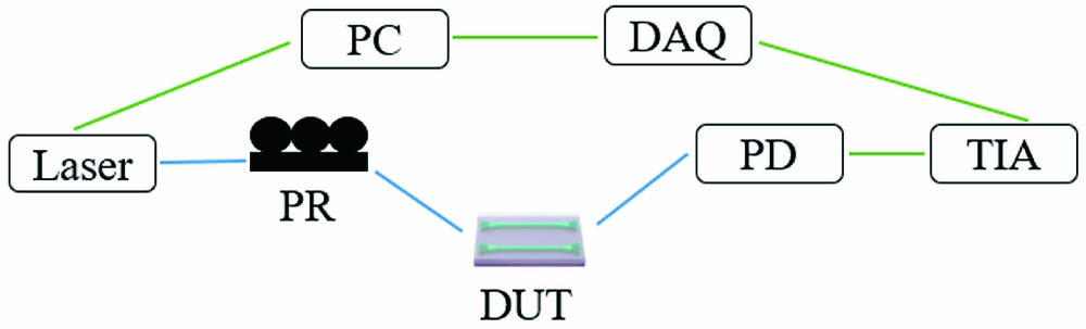
As a promising spectral window for optical communication and sensing, it is of great significance to realize on-chip devices at the 2 µm waveband. The development of the 2 µm silicon photonic platform mainly depends on the performance of passive devices. In this work, the passive devices were fabricated in the silicon photonic multi-project wafer process. The designed micro-ring resonator with a 0.6 µm wide silicon ridge waveguide based on a 220 nm silicon-on-insulator platform achieves a high intrinsic quality factor of . The propagation loss is calculated as 1.62 dB/cm. In addition, the waveguide crossing, multimode interferometer, and Mach–Zehnder interferometer were demonstrated at 2 µm with good performances.
silicon photonics integrated photonics grating coupler multimode interferometer waveguide crossing Chinese Optics Letters
2021, 19(7): 071301
重庆大学光电工程学院光电技术及系统教育部重点实验室, 重庆 400044
利用真空抽滤法制备出具有宽频域吸光性能,且可应用于金属和塑料等多种环境的自支持碳纳米管薄膜(CNF);利用表面活性剂辅助制备了稳定的碳纳米管分散液,利用真空抽滤法在混合纤维素滤膜上得到了不同厚度的碳纳米管薄膜,并利用氙灯加热法实现了薄膜的完美分离。结果表明:碳纳米管分散液经真空抽滤后可在滤膜上形成具有纠缠交错呈平面网状结构的连续均匀各向同性薄膜,薄膜厚度与抽滤碳纳米管沉积量成正比关系;薄膜的光吸收率随着方阻的增大而增大,实验观察结果与用电磁场理论分析结果相符;350~2500 nm波段宽频域的光吸收率为94%~98%,并具有一定的提高空间。
薄膜 碳纳米管薄膜 真空抽滤法 吸光性能 电磁场理论 中国激光
2013, 40(s1): s107001


